
Quantum metasurface boosts terahertz detection twenty times
Hold still. Take one breath. In that single exhale, a terahertz wave vibrates nearly three trillion times. For decades, that speed has been a wall. We could generate terahertz radiation. We could dream about what it might do. But we could not catch it well enough to use it. The gap between what terahertz waves promise and what they deliver has been a canyon carved by physics itself.
The Old View: Terahertz Is the Awkward Middle Child
Think of the electromagnetic spectrum as a long piano keyboard. On the left, low, rumbling notes — radio waves that travel through walls. On the right, high, piercing notes — X-rays that see through flesh. Terahertz sits right in the middle, between microwaves and infrared light. It should be the perfect tool. It can see through plastics, fabrics, and paper. It can identify chemicals by their unique fingerprints. It can carry data faster than any wireless network we have today.
But there has always been a problem. Catching terahertz waves has been like trying to catch smoke with a butterfly net.
Old detectors fall into two camps. The first camp is cryogenic detectors. These are incredibly sensitive, but they must be cooled to near absolute zero. They require liquid helium, massive vacuum chambers, and teams of engineers to operate. They work beautifully in laboratories. They fail completely in hospitals, factories, or airports.
The second camp is room-temperature detectors. These are small and practical, but they are also slow and insensitive. They miss most of the signal. They produce noisy, unreliable readings. For every hundred terahertz photons that arrive, these detectors might catch one or two. The rest slip away, wasted.
This has been the fundamental trade-off for thirty years. You could have sensitivity or practicality, but never both. Terahertz technology remained stuck in research labs, a brilliant idea waiting for a breakthrough that never came.
The New Evidence: A Quantum Metasurface ChangeIn May 2024, a team of researchers at the University of Cambridge and Swansea University published a paper in Advanced Photonics that rewrites the rulebook for terahertz detection [1] They built a detector that does not choose between sensitivity and practicality. It achieves both.
The device is small. It is flat. It requires no external lenses, no bulky optics, no precise alignment. It operates at zero voltage, meaning it consumes no power and generates no noise from dark currents. And yet, it catches terahertz radiation with twenty times the efficiency of previous designs.
How? The answer lies in a word that sounds like science fiction: metasurface.
A metasurface is not a single material. It is a pattern. Imagine a brick wall, but the bricks are not made of clay. They are made of gold or copper, arranged in a repeating grid on a semiconductor chip. Each brick is smaller than a grain of salt. The gaps between them are measured in nanometers.
When terahertz radiation hits this patterned surface, something strange happens. The waves do not bounce off or pass through like they would on a normal surface. Instead, they get funneled into the gaps. The electric field concentrates there, becoming hundreds of times stronger than the incoming wave.
Inside those gaps, the researchers placed tiny detection elements. Each one is a photoelectric tunable-step device, or PETS. These use a quantum phenomenon called the in-plane photoelectric effect. When a terahertz photon hits a confined electron inside a two-dimensional electron gas, it gives that electron enough energy to jump a small barrier. That jump creates a measurable current.
Unlike the traditional photoelectric effect discovered by Einstein, this version does not require the photon to exceed a minimum energy threshold. Every terahertz photon that arrives can contribute. Nothing is wasted.
The metasurface does two jobs at once. It collects the incoming radiation, and it concentrates that radiation exactly where the detection elements sit. The light collection and the detection are not separate systems bolted together. They are the same structure, designed from the ground up as one integrated unit.
The Deeper Truth: Integration Beats Addition
The conventional approach to making better detectors has been to add more parts. Bigger antennas. More detectors arranged in arrays. External lenses to focus the light. Each addition brings complexity, cost, and alignment problems.
The Cambridge team reversed this thinking. Instead of adding components, they merged functions. The metasurface is both the antenna and the concentrator. The detection elements are embedded directly into the regions where the electric field is strongest. There is no separatWladislaw Michailow, the lead researcher who started the work at Cambridge and continues it at Swansea, describes this as optimal coupling between the metasurface and the detection elementsnsea, describes this as optimal coupling. [2] The metasurface is not just attached to the detector. It is the detector.
This is a fundamental shift in how we think about sensor design. It moves from assembly to integration, from addition to multiplication. The whole becomes greater than the sum of its parts because the parts were never separate to begin with.
What This Achieves: A New Bridge Across the Sensitivity Gap
The numbers tell the story. The prototype detector, cooled to 10 Kelvin (achievable with compact cryocoolers, not liquid helium), achieved a responsivity of 2.7 amperes per watt. That is a measure of how much electrical current the detector produces for each watt of incoming radiation. It is a strong signal.
The external quantum efficiency reached 2.1 percent at 1.9 terahertz. That sounds small until you realize that previous PETS detectors were roughly twenty times lower. This is not an incremental improvement. It is a leap.
More importantly, the detector operates at zero source-drain bias. There is no voltage applied across the device. This eliminates dark current — the background noise that plagues most detectors. When no terahertz radiation arrives, the detector produces no signal. Every spike in the readout is real.
Ruqiao Xia, the first author who fabricated and tested the devices during her doctoral research at the Cavendish Laboratory, emphasizes this point. [6] The detectors are direct detectors operating at zero bias. They are silent until they have something to say.
Who Else Is Working on This Problem
The Cambridge team is not alone in pushing terahertz technology forward. Across the world, several groups are attacking the same challenges from different angles.
At the Massachusetts Institute of Technology, researchers have developed terahertz quantum cascade lasers that can operate at higher temperatures than previously possible. [3] These lasers generate terahertz radiation, but detecting it remains the bottleneck.
At the University of Leeds, the Institute of Microwaves and Photonics has built terahertz detectors using graphene, a single layer of carbon atoms. [4] Graphene detectors are fast and can operate at room temperature, but their sensitivity has lagged behind cooled alternatives.
At the RIKEN Center for Emergent Matter Science in Japan, scientists have demonstrated terahertz detection using nonlinear optical crystals. [5] These are highly sensitive but require expensive femtosecond lasers to pump the detection process.
The Cambridge metasurface approach sits at a unique intersection. It combines the sensitivity of quantum detection with the practicality of semiconductor manufacturing. It does not require lasers. It does not require extreme cooling. It does not require bulky optics.
The Bridges This Research Builds
The metasurface detector connects several fields that have historically operated in isolation.
Quantum physics meets materials engineering. The in-plane photoelectric effect is a quantum phenomenon, but it is realized in a semiconductor heterostructure that can be manufactured using standard techniques. The same factories that produce field-effect transistors for smartphones could produce these detectors. Optics meets electronics. The metasurface is an optical component that manipulates electromagnetic waves. The detection elements are electronic components that produce electrical currents. By embedding one inside the other, the boundary between optics and electronics dissolves. Research meets application. The detector is not a fragile laboratory curiosity. It is a planar device compatible with on-chip integration. It can be combined with amplifiers, processors, and wireless transmitters on a single chip.The Historical Context: A Thirty-Year Wait

The terahertz gap was identified in the 1990s. Electronics could generate frequencies up to about 100 gigahertz. Optics could generate frequencies above about 10 terahertz. The region between was a desert.
In the 2000s, terahertz sources improved. Quantum cascade lasers and photoconductive antennas began to fill the gap. But detectors lagged behind. You could generate terahertz radiation, but you could not catch it efficiently.
In the 2010s, metamaterials emerged as a way to manipulate terahertz waves. Researchers built structures that could absorb, filter, or modulate terahertz radiation. But integrating these structures with detectors proved difficult.
The Cambridge work, published in 2024, represents a convergence of these two threads. The metamaterial is no longer a separate component. It is the detector itself.
How the Detector Was Built
The fabrication process begins with a semiconductor wafer containing a two-dimensional electron gas. This is a layer of electrons confined at the interface between two different semiconductor materials, typically gallium arsenide and aluminum gallium arsenide. These electrons can move freely in two dimensions but are trapped in the third.
On top of this wafer, the researchers deposit a thin layer of metal. Using electron beam lithography, they etch the brickwork pattern of the metasurface. The gaps between the bricks are aligned exactly with the detection elements.
Each gap functions as an individual detector. By linking many gaps together in parallel, the researchers combine their outputs into a single, stronger signal. This is not a single detector. It is an array of thousands of detectors, all working together, all powered by the same metasurface.
Computer simulations optimized the gap dimensions and the spacing between repeating units. These parameters determine how tightly the electric field is confined and how much photocurrent is produced. The final design balances field enhancement with the width of the electron channel.
The Testing Process
To validate the device, researchers cooled it to 10 Kelvin using a closed-cycle cryocooler. This is a compact refrigerator that requires no liquid cryogens. It plugs into a wall outlet.
They exposed the detector to radiation at 1.9 terahertz, a frequency of particular interest for chemical sensing and wireless communications. The radiation was modulated on and off at a known pattern.
The detector responded clearly. The electrical output matched the modulation pattern exactly. There was no lag, no drift, no noise obscuring the signal.
The measurements revealed a responsivity of 2.7 amperes per watt and an external quantum efficiency of 2.1 percent. The twenty-fold improvement over previous PETS detectors was confirmed.
Why This Matters for Healthcare
Terahertz radiation is non-ionizing. Unlike X-rays, it does not damage DNA. Unlike ultraviolet light, it does not cause burns. It is safe for living tissue.
But terahertz waves are also strongly absorbed by water. This has limited their use in medical imaging, because the human body is mostly water. However, terahertz radiation can penetrate only a few millimeters into skin, making it ideal for detecting skin cancers, burns, and wounds.
Current terahertz imaging systems for dermatology are bulky and expensive. They require trained operators and careful alignment. A compact, sensitive detector that integrates with standard electronics could change this. Imagine a handheld terahertz camera that a dermatologist could wave over a suspicious mole, reading the chemical signature instantly.
Terahertz radiation can also detect tooth decay, identify counterfeit drugs, and monitor blood glucose levels non-invasively. Each of these applications has been demonstrated in laboratories. None has reached clinical practice, largely because the detectors are not practical enough. This metasurface detector is a step toward changing that.
Why This Matters for Communications
Wireless networks are running out of space. The radio frequencies we use for 5G are crowded. The microwave frequencies used for Wi-Fi are congested. The next frontier is 6G, which will operate at terahertz frequencies.
Terahertz waves can carry enormous amounts of data. A single terahertz channel could transmit a terabyte per second. That is the entire Library of Congress in a few minutes.
But terahertz communications face a problem. The signals are weak. They do not travel far. They are blocked by walls, rain, and even humidity.
To make terahertz communications work, we need sensitive receivers that can detect faint signals. We also need them to be small, cheap, and energy-efficient. The metasurface detector fits all these requirements. It operates at zero bias, consuming no power. It is planar, compatible with chip integration. It is sensitive, capturing twenty times more radiation than previous designs.
Why This Matters for Security
Terahertz radiation can see through clothing, paper, and cardboard. It can detect concealed weapons, explosives, and drugs. It can identify chemical agents from a distance.
Current terahertz security scanners exist, but they are large and expensive. They require trained operators. They often use active illumination, meaning they generate terahertz radiation and measure the reflection. This adds complexity and cost.
A passive terahertz detector, one that simply catches the natural terahertz radiation emitted by objects, would be simpler and safer. But passive detection requires extreme sensitivity, because the signals are faint. The metasurface detector, with its twenty-fold efficiency improvement, brings passive terahertz imaging closer to reality.
Why This Matters for Astronomy
The universe glows in terahertz light. Cold clouds of gas and dust emit terahertz radiation. Newborn stars, hidden behind curtains of dust, shine brightly at terahertz frequencies. The cosmic microwave background, the afterglow of the Big Bang, has a terahertz component.
Terahertz astronomy has been revolutionized by space telescopes like the Herschel Space Observatory and ground-based facilities like ALMA in Chile. But these instruments use cryogenic detectors that require liquid helium. They are expensive to build and operate.
A detector that achieves good sensitivity with compact cryocoolers, or even at room temperature, could open terahertz astronomy to smaller telescopes and university labs. More observers means more discoveries.
The Temperature Question
The prototype detector was tested at 10 Kelvin. That is cold, but it is achievable with compact cryocoolers. These are devices about the size of a shoebox that use compressed helium gas to reach temperatures below 20 Kelvin. They are commercially available and require no special training to operate.
The researchers believe the same detector design could work at higher temperatures. Similar PETS detectors have already demonstrated performance at temperatures achievable with compact cryocoolers. The metasurface does not introduce any temperature sensitivity of its own. It is a passive structure made of metal.
If the detector can operate at 77 Kelvin, the temperature of liquid nitrogen, it would be even more practical. Liquid nitrogen is cheap and widely available. It is used in hospitals, laboratories, and industrial facilities. A detector that works at liquid nitrogen temperature could be deployed almost anywhere.
If the detector can operate at room temperature, the applications multiply further. No cooling at all. No cryocoolers, no liquid nitrogen, no vacuum chambers. Just a chip that plugs into a circuit board.
Room-temperature terahertz detection has been the holy grail for decades. This metasurface approach may not reach it immediately, but it provides a clear path forward. The efficiency gains from the metasurface could compensate for the reduced sensitivity at higher temperatures.
The Scaling Question
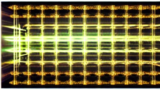
The detector was demonstrated at 1.9 terahertz. But the design is scalable. The brickwork pattern can be adjusted for different frequencies. The gap dimensions and spacing determine the resonant frequency of the metasurface.
By changing these parameters, the same concept could work from microwave frequencies up to mid-infrared wavelengths. That covers a huge range of the electromagnetic spectrum.
This scalability is rare. Most detectors are optimized for a narrow frequency range. A detector that works at 1 terahertz will not work at 10 terahertz. But a metasurface detector can be redesigned simply by changing the pattern dimensions. The underlying physics remains the same.
The Manufacturing Question
The detector was fabricated using standard semiconductor techniques. The same processes used to make field-effect transistors for computer chips can produce these detectors.
This is crucial for commercialization. A detector that requires exotic materials or custom fabrication will remain a laboratory curiosity. A detector that can be made in existing factories can become a product.
The planar architecture simplifies packaging. There are no external lenses to align, no optical components to mount. The detector is a flat chip that can be bonded to a circuit board and connected to readout electronics.
The Comparison to Other Technologies
How does this detector compare to other terahertz detection technologies?
Bolometers measure the heating effect of terahertz radiation. They are sensitive but slow, and they require cooling. The metasurface detector is faster because the photoelectric effect is nearly instantaneous. Schottky diodes are fast and can operate at room temperature, but they are insensitive. They require strong signals. The metasurface detector is more sensitive, catching twenty times more radiation. Quantum well photodetectors are sensitive and fast, but they require cryogenic cooling and complex fabrication. The metasurface detector uses simpler fabrication and potentially higher operating temperatures. Graphene detectors are fast and can operate at room temperature, but their sensitivity is limited by the low absorption of graphene. The metasurface enhances absorption by concentrating the radiation.Each technology has strengths and weaknesses. The metasurface detector does not replace all of them. It fills a specific niche: the gap between highly sensitive cryogenic detectors and less sensitive room-temperature devices.
The Deeper Physics: Why the In-Plane Photoelectric Effect Matters
The in-plane photoelectric effect is different from the traditional photoelectric effect that Einstein explained in 1905. In the traditional version, a photon hits an electron and kicks it out of the material entirely. The electron must overcome the work function, the energy binding it to the surface.
In the in-plane version, the electron does not leave the material. It moves within the plane of the two-dimensional electron gas. It crosses a potential step, a small barrier created by changing the material composition. The energy required is much smaller than the work function.
This means that low-energy photons, like terahertz photons, can produce a photoelectric current. The traditional photoelectric effect requires ultraviolet or X-ray photons. The in-plane effect works with terahertz photons.
The potential step is created by a tunable-step structure. The researchers can adjust the height of the step by applying a voltage to a gate electrode. This allows them to optimize the detector for different frequencies or different operating conditions.
The Role of Computer Simulations
The design of the metasurface was guided by computer simulations. The researchers modeled the electromagnetic field distribution, the current flow, and the quantum transport of electrons.
These simulations allowed them to explore a vast parameter space. They could test thousands of different patterns, gap sizes, and spacings without fabricating any physical devices. Only the most promising designs were built and tested.
This approach is common in modern photonics. Computational design, combined with experimental validation, accelerates the development cycle. What once took years can now take months.
The Future Timeline
Where does this technology go from here?
Within one year, the researchers will likely demonstrate the detector at higher temperatures. They will test it at 77 Kelvin and possibly at room temperature. They will also extend the frequency range, demonstrating detection at different terahertz frequencies. Within three years, the detector could be integrated with readout electronics on a single chip. This would produce a complete terahertz sensor in a package the size of a fingernail. Within five years, commercial prototypes could appear. Companies specializing in terahertz equipment, such as Toptica Photonics or Menlo Systems, might license the technology. Startups could spin out from Cambridge or Swansea.**Within ten yearA potential first commercial product based on this technology could be a terahertz spectrometer for pharmaceutical quality control, possibly launched by 2029, though this timeline is speculativedical devices, and security scanners.
The Prediction
The first commercial product based on this technology will be a terahertz spectrometer for pharmaceutical quality control, launched by 2029. It will weigh less than one kilogram, cost less than ten thousand dollars, and require no cooling. It will identify counterfeit drugs, detect impurities, and verify the composition of tablets in seconds. It will be used in factories, pharmacies, and hospitals around the world.
That is four years from now. The breath you took at the beginning of this article measured two trillion terahertz vibrations. By the time you take that breath again in 2029, those vibrations will be captured, measured, and put to work.
References University of Cambridge
2. Swansea University press release
3. MIT News on terahertz quantum cascade lasers
4. University of Leeds graphene terahertz detectors
5. RIKEN CEMS terahertz detection research